
News
What Is SMT Assembly and How Does It Work?
Smt Assembly is the process of mounting electronic components directly onto a printed circuit board, often using automated equipment. It enables manufacturers to place tiny resistors, capacitors, and integrated circuits with speed and repeatability. The global context is expanding: the WSTS Spring 2024 Forecast projected semiconductor sales of $611.2 billion in 2024, rising to $687.4 billion in 2025. These figures describe chip sales, not SMT production, but they show the scale of the component ecosystem that assembly lines serve.
A typical line begins with solder paste printed through a stencil onto copper pads. A placement machine then positions components, sometimes smaller than a grain of rice. The board passes through a reflow oven, where controlled heat melts the paste and forms electrical joints. Inspection systems check alignment and solder quality. The details matter. IPC J-STD-001 and IPC-A-610 provide widely used requirements and acceptance criteria for soldered assemblies. Yet no standard replaces process control: paste condition, board design, component handling, and oven settings can all affect results. A fast line can still produce defects. That is an easy point to overlook. Understanding what happens at each stage makes it easier to assess quality, troubleshoot failures, and choose suitable manufacturing controls.
What Surface-Mount Technology Assembly Is
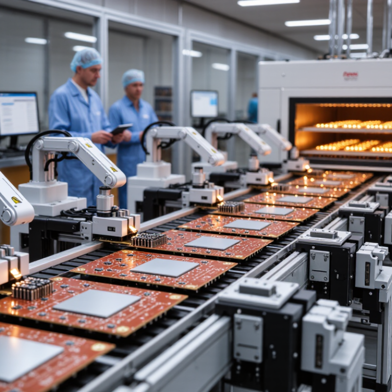
Surface-mount technology (SMT) assembly is the process of attaching electronic components directly to conductive pads on a circuit board. Unlike traditional through-hole assembly, most SMT components do not need leads inserted through drilled holes. This allows compact layouts and supports automated production. Small parts, tight spacing.
A typical line begins with solder paste, a mix of fine solder particles and flux, applied through a stencil onto board pads. A placement machine then positions components, sometimes smaller than a grain of rice. The board passes through a reflow oven, where controlled heat melts the paste and forms solder joints. Temperature profiles matter: too much heat can damage parts, while too little may leave weak connections.
After cooling, inspection checks component position and solder quality. Cameras can identify misalignment or visible defects; X-ray inspection can help examine joints hidden beneath certain components. SMT is efficient, but it is not foolproof. Board cleanliness, paste volume, component handling, and oven settings all affect results. A board may look tidy and still contain a weak joint, so inspection methods should match the design and its reliability needs.

The Main Materials and Equipment Used in SMT
SMT assembly depends on a small set of materials working together. Solder paste joins component terminals to copper pads on the printed circuit board. Its metal powder, flux, and particle size affect print quality and joint formation. For lead-free assemblies, SAC305 contains 96.5% tin, 3.0% silver, and 0.5% copper, as designated in IPC J-STD-006. The exact paste choice still depends on component pitch, board finish, and thermal limits. Small details matter.
The core equipment follows the paste from deposition to inspection. A stencil printer presses paste through a thin metal stencil; IPC-7525 provides guidance for stencil design. Solder paste inspection checks deposit area, height, and volume before components are placed. A pick-and-place machine positions parts, then a reflow oven heats the board according to the paste supplier’s profile. Automated optical inspection can flag shifted components or visible solder defects. It cannot confirm every hidden joint. That limitation is easy to overlook. Board material, stencils, feeders, and maintenance also influence results, so a stable process needs careful checks, not just fast machines.
Solder Paste Powder Sizes Used in SMT Assembly
Solder paste combines metal powder with flux and is applied using a stencil printer. Finer powder can support printing for smaller component features, while the suitable type depends on the stencil aperture, component pitch, and process requirements. Particle-size ranges shown are commonly used specifications; check the solder paste supplier’s datasheet for the exact range.
How the PCB Is Prepared and Solder Paste Is Applied
Before SMT assembly, the bare PCB needs a clean, stable surface. Dust, skin oils, and moisture can interfere with solder wetting. Operators inspect pads, check board support, and align stencil fiducials with PCB marks. Small alignment errors matter. A fine-pitch pad can be partly blocked by a misplaced stencil. Board warpage deserves attention, too; a board may look flat but lift during printing.
Solder paste is pressed through stencil apertures onto the pads, usually with a controlled squeegee pass. IPC J-STD-005 classifies solder-powder sizes: Type 3 particles measure 25–45 micrometers, while Type 4 measures 20–38 micrometers. These are specification ranges, not guarantees of print quality. Smaller particles can suit tighter apertures, but paste choice must match the stencil and component pitch. After printing, solder paste inspection measures deposit area, height, and volume. A clean-looking board can still have uneven deposits. That step is easy to rush. Process records should note actual inspection results, not only printer settings; otherwise, a recurring defect can hide in plain sight.
| Step | Preparation or Process | What Happens | Typical Quality Check |
|---|---|---|---|
| 1 | PCB and assembly data review | The board layout, component locations, solder-mask openings, and manufacturing files are checked before production. | Confirm that the board data, component list, and stencil data correspond to the same design revision. |
| 2 | Bare-board inspection | The PCB is checked for visible damage, contamination, and issues that could affect component placement or soldering. | Inspect board edges, pads, solder-mask openings, and fiducial marks. |
| 3 | Board cleaning and handling | Dust, fingerprints, and other contaminants are controlled because they can interfere with solder paste or solder-joint formation. | Keep the board surface clean and dry; use handling procedures suited to the board and process. |
| 4 | Panel loading and alignment | A single PCB or production panel is secured in the printer. Fiducials help the machine align the stencil apertures with the PCB pads. | Check that the board is seated securely and that the alignment system can detect the fiducials. |
| 5 | Stencil selection and setup | A metal stencil with openings corresponding to the PCB pads is positioned over the board. Stencil thickness and aperture design influence the amount of paste deposited. | Verify stencil identity, orientation, alignment, and condition before printing. |
| 6 | Solder paste preparation | Solder paste is brought to the condition specified by its supplier and handled according to its storage and use instructions. | Check the paste type, usable life, and handling requirements; avoid introducing moisture or contamination. |
| 7 | Solder paste printing | A squeegee moves paste across the stencil, forcing it through the apertures onto the corresponding PCB pads. The stencil is then separated from the board. | Look for consistent deposits, correct pad coverage, and minimal smearing or bridging between adjacent pads. |
| 8 | Post-print inspection | The printed board is inspected before component placement. Automated solder paste inspection may measure deposit area, height, volume, and position. | Detect missing, insufficient, excessive, or misaligned paste deposits and correct printing problems early. |
| 9 | Component placement and reflow | After printing is accepted, surface-mount components are placed onto the paste. The board is later heated in a reflow oven so the paste melts and forms solder joints. | Check placement accuracy and use a reflow profile appropriate for the board, components, and solder paste. |
How Components Are Placed and Soldered onto the Board
SMT assembly starts with solder paste, a gray mixture of tiny solder particles and flux. A metal stencil is aligned over the circuit board, and a blade spreads paste through openings onto the component pads. The stencil must sit flat. Small shifts can leave paste misplaced or uneven, creating weak joints or shorts.
A pick-and-place machine then uses programmed coordinates and a camera to position components. Its nozzle lifts each part from a feeder and sets it onto the paste. Tiny resistors may be smaller than a grain of rice, while chips have marked orientations that must match the board layout. Placement is precise, not infallible. A skewed part or reversed polarity can still slip through, especially when setup data or board references are wrong.
The populated board travels through a reflow oven, where controlled heating melts the solder and bonds each component to its pads. Heat matters. The temperature profile must suit the board and components; too much heat can damage parts, while too little may leave unreliable joints. After cooling, optical inspection checks alignment, solder shape, and missing parts. Some defects are difficult to see, so inspection results may call for process adjustments. A stable line helps, but it does not remove the need to question its settings.
How the Finished Assembly Is Inspected and Tested
After reflow, inspection checks whether solder joints, component positions, and polarity match the assembly requirements. Automated optical inspection (AOI) uses cameras to flag shifted parts, missing components, and visible solder defects. A bright image helps, but it cannot reveal every hidden joint.
For components with concealed connections, such as bottom-terminated packages, X-ray inspection can show solder-ball shape and bridging beneath the package. IPC-A-610 sets acceptance criteria across three product classes, so inspectors must apply the class specified for the assembly. That detail matters. A visually neat board is not automatically acceptable. IPC-9261 also uses defects per million opportunities (DPMO) to track process performance; this metric can help teams compare defect trends over time, but it does not replace inspection of the actual board.
Electrical checks add another layer. In-circuit testing can find opens, shorts, and incorrect component values, while functional testing checks whether the powered assembly behaves as intended. Test results should link to board identity and inspection records, making recurring faults easier to trace. Still, no single test catches everything. A test fixture can miss a fault outside its coverage, and that limitation deserves review. Teams should use failure data to refine inspection points, not just rerun the same checks.